CMOS Logic and their characteristics:
CMOS stands for “Complementary metal Oxide Semiconductor”. It is also known as “complimentary-symmetry metal Oxide Semiconductor COS-MOS”.
It is widely used in the integration of chips (ICs). It is used in Computer memories like RAM, ROM, EEPROM, cell phones, microprocessors and microcontrollers.
Structure of CMOS:
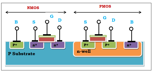
The power dissipation and consumption is very less in CMOS and it is faster, so it is widely used than the bipolar circuits. CMOS consists of P- channel MOSFET (PMOS) and N-channel MOSFET (NMOS).
 |
| Structure of CMOS |
N-channel MOSFET (NMOS):
NMOS is built over a P substrate. Source and drain are made up of n type material. Here the majority carriers are electrons. NMOS is faster than the PMOS, because the electrons which is the majority carriers travel twice the time faster than the holes. It conducts when the voltage is high and does not conduct when the voltage is low.
P- Channel MOSFET (PMOS):
PMOS is built over an N substrate. Source and drain are made up of p type material. Here the majority carriers are holes. PMOS is slower than the NMOS. It conducts when the voltage is low and does not conduct when the voltage is high.
Working of CMOS:
 |
| Working of CMOS |
Both NMOS and PMOS together design the logic function. Same input voltage is used to turn ON one MOSFET and turn OFF other MOSFET. So there is no need of pull up resistor in CMOS.
NMOS is arranged in the pull down network between the output and the ground. PMOS is arranged in the pull up network. This pull up and pull down network is arranged in such a way that when one network is ON, the other network will be OFF.
CMOS Inverter:
 |
| CMOS inverter |
NMOS is connected with VSS or ground and PMOS is connected with VDD. When the high voltage VDD is given at the input of the inverter, the PMOS will be an open circuit and the NMOS will be switched OFF. So the output will be pulled down to the ground or VSS.
When the low voltage VSS is given at the input of the inverter, the PMOS will be ON and the NMOS will be switched OFF. So the output will be pulled up to VDD.
 |
| CMOS inverter table |
Characteristics of CMOS:
Fan in and Fan out:
Number of inputs and outputs connected to the gate, which does not affect the usual performance and does not degrade the voltage. Fan in and Fan out is usually 10 for CMOS.
Power dissipation:
It is amount of power the device needs. It is the product of the voltage which is supplied and current needed to produce the output. It is measured in mW. Usually it is 10mW at 1MHZ and 0.1mW at 100KHZ.
Noise Margin:
It is the amount of noise voltage allowed at the input and it should not affect the output. The noise margin in CMOS is 45% of the supply voltage. It is usually 2.25V for 5V input.
Propagation Delay:
It is the time taken from applying the input to the output produced. It is normally 25 to 150ns.
Advantages of CMOS:
• Power consumption is less
• Large fan-out capability
• High noise immunity and noise margin
• Power dissipation is low
• Faster than NMOS
Disadvantages of CMOS:
• Manufacturing cost is high
• Propagation delay is higher than TTL and ECL
Applications of CMOS:
• Analog to digital converter
• Image sensors
• Amplifiers
• Static RAM
• Registers
• Microchip
• Microprocessors and microcontrollers
• Transceivers


0 Comments