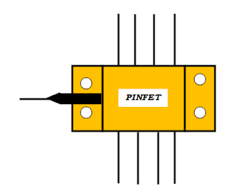
What is PINFET?
PINFET stands for P type- intrinsic- N type Field Effect transistor. It is a integration of PIN Photodiode and FET in a single IC. PIN diode converts light energy into an electrical signal and it is designed to operate in a reverse biased condition. Field Effect Transistor is a voltage controlled device. The voltage which is given in the gate terminal as input controls the current passing through it.
Construction of PINFET:
| Construction of PINFET |
PINFET is the combination of InGaAs PIN Photodiode and InGaAs FET. The construction process includes the following
1) Metal Organic chemical vapour deposition(MOCVD):
By using this method PINFET is fabricated over semi insulating InGaAs substrate.
2) Chloride Vapour Phase epitaxy(VPE):
By this process InGaAs layer of low concentration of electrons is grown above the substrate.
3) Atmospheric pressure metal organic chemical vapour deposition technique:
By this method silicon interface layer is grown over the InGaAs layer.
4) Ion Implantation: By this process which is done in series the FET is formed.
5) Deposition and diffusion: By this process PIN diode is formed.
Working of PINFET:
| Working of PINFET |
It consists of three regions P region, I region and N region. P region and N region are heavily doped regions and they are used as Ohmic contacts. A wider intrinsic silicon layer is sandwiched between two heavily doped layers and it absorbs the light photons which forms the electron hole pairs. The intrinsic layer is highly resistive and it increases the width of the depletion region. In normal diode only voltage is used to form the current but in PINFET both voltage and light is used to form the current.
When reversed biased the majority carriers in highly doped P type and N type does not conduct current so the charge carriers move away from the junction and the intrinsic layer is undoped which does not have majority charge carriers. So the width of the depletion region increases. When the light is incident on the PINFET the wider intrinsic layer absorbs the light energy and forms large number of electron hole pairs.
The free electrons which are generated in the intrinsic region move towards the N region and the free holes move towards the P region and these charge carriers are attracted towards the positive and negative terminals. Thus current is formed due to the movement of these charge carriers.
The intrinsic layer acts as a dielectric layer and highly doped P and N layer acts as electrodes in the capacitor. Since the distance between the electrodes are very large, the capacitance is very low and thus the noise is very low.
Advantages of PINFET:
- Wide bandwidth
- Low noise
- High sensitivity to light
- Low sensitivity to temperature
- Low cost
- Small size
- Long lifetime
Disadvantages of PINFET:
- It always operates in reverse biased condition
- It is a light sensitive device
- Should not exceed the working temperature limit specified by the manufacturer.
Applications
- PINFET is mainly used as a photo receiver in optical communication because of its low noise and high speed.
- Used in optical Sensor systems.
- Used as repeaters in telecommunication


0 Comments